- 您现在的位置:买卖IC网 > Sheet目录364 > SST25VF020B-80-4C-QAE-T (Microchip Technology)IC FLASH SER 2MB 80MHZ SPI 8WSON
�� �
�
�2� Mbit� SPI� Serial� Flash�
�A� Microchip� Technology� Company�
�SST25VF020B�
�Data� Sheet�
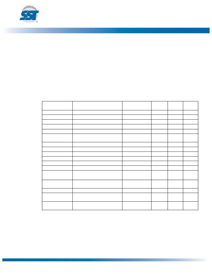
�Instructions�
�Instructions� are� used� to� read,� write� (Erase� and� Program),� and� configure� the� SST25VF020B.� The�
�instruction� bus� cycles� are� 8� bits� each� for� commands� (Op� Code),� data,� and� addresses.� Prior� to� execut-�
�ing� any� Byte-Program,� Auto� Address� Increment� (AAI)� programming,� Sector-Erase,� Block-Erase,� Write-�
�Status-Register,� or� Chip-Erase� instructions,� the� Write-Enable� (WREN)� instruction� must� be� executed�
�first.� The� complete� list� of� instructions� is� provided� in� Table� 6.� All� instructions� are� synchronized� off� a� high�
�to� low� transition� of� CE#.� Inputs� will� be� accepted� on� the� rising� edge� of� SCK� starting� with� the� most� signif-�
�icant� bit.� CE#� must� be� driven� low� before� an� instruction� is� entered� and� must� be� driven� high� after� the� last�
�bit� of� the� instruction� has� been� shifted� in� (except� for� Read,� Read-ID,� and� Read-Status-Register� instruc-�
�tions).� Any� low� to� high� transition� on� CE#,� before� receiving� the� last� bit� of� an� instruction� bus� cycle,� will�
�terminate� the� instruction� in� progress� and� return� the� device� to� standby� mode.� Instruction� commands�
�(Op� Code),� addresses,� and� data� are� all� input� from� the� most� significant� bit� (MSB)� first.�
�Table� 6:� Device� Operation� Instructions�
�Address�
�Dummy�
�Data�
�Instruction�
�Description�
�Op� Code� Cycle� 1�
�Cycle(s)� 2� Cycle(s)� Cycle(s)�
�Read�
�High-Speed� Read�
�Read� Memory�
�Read� Memory� at� higher� speed�
�0000� 0011b� (03H)�
�0000� 1011b� (0BH)�
�3�
�3�
�0�
�1�
�1� to� ?�
�1� to� ?�
�4� KByte� Sector-Erase� 3� Erase� 4� KByte� of� memory� array�
�0010� 0000b� (20H)�
�3�
�0�
�0�
�32� KByte� Block-Erase� 4�
�Erase� 32� KByte� block� of� memory� array� 0101� 0010b� (52H)�
�3�
�0�
�0�
�64� KByte� Block-Erase� 5� Erase� 64� KByte� block� of� memory� array� 1101� 1000b� (D8H)�
�3�
�0�
�0�
�Chip-Erase�
�Erase� Full� Memory� Array�
�0110� 0000b� (60H)� or�
�0�
�0�
�0�
�1100� 0111b� (C7H)�
�Byte-Program�
�To� Program� One� Data� Byte�
�0000� 0010b� (02H)�
�3�
�0�
�1�
�AAI-Word-Program� 6� Auto� Address� Increment� Programming� 1010� 1101b� (ADH)�
�3�
�0�
�2� to� ?�
�RDSR� 7�
�RDSR1�
�EWSR�
�WRSR�
�WREN�
�WRDI�
�RDID� 8�
�Read-Status-Register�
�Read-Status-Register� 1�
�Enable-Write-Status-Register�
�Write-Status-Register�
�Write-Enable�
�Write-Disable�
�Read-ID�
�0000� 0101b� (05H)�
�0011� 0101b� (35H)�
�0101b� 0000b� (50H)�
�0000� 0001b� (01H)�
�0000� 0110b� (06H)�
�0000� 0100b� (04H)�
�1001� 0000b� (90H)� or�
�0�
�0�
�0�
�0�
�0�
�0�
�3�
�0�
�0�
�0�
�0�
�0�
�0�
�0�
�1� to� ?�
�1� to� ?�
�0�
�1� or� 2�
�0�
�0�
�1� to� ?�
�1010� 1011b� (ABH)�
�JEDEC-ID�
�JEDEC� ID� read�
�1001� 1111b� (9FH)�
�0�
�0�
�3� to� ?�
�EBSY�
�Enable� SO� to� output� RY/BY#� status� 0111� 0000b� (70H)�
�0�
�0�
�0�
�during� AAI� programming�
�DBSY�
�Disable� SO� as� RY/BY#�
�1000� 0000b� (80H)�
�0�
�0�
�0�
�status� during� AAI� programming�
�T6.0�
�25054�
�1.�
�2.�
�3.�
�4.�
�5.�
�6.�
�One� bus� cycle� is� eight� clock� periods.�
�Address� bits� above� the� most� significant� bit� of� each� density� can� be� V� IL� or� V� IH� .�
�4KByte� Sector� Erase� addresses:� use� A� MS� -A� 12,� remaining� addresses� are� don’t� care� but� must� be� set� either� at� V� IL� or� V� IH.�
�32KByte� Block� Erase� addresses:� use� A� MS� -A� 15,� remaining� addresses� are� don’t� care� but� must� be� set� either� at� V� IL� or� V� IH.�
�64KByte� Block� Erase� addresses:� use� A� MS� -A� 16,� remaining� addresses� are� don’t� care� but� must� be� set� either� at� V� IL� or� V� IH.�
�To� continue� programming� to� the� next� sequential� address� location,� enter� the� 8-bit� command,� ADH,� followed� by� 2� bytes� of�
�data� to� be� programmed.� Data� Byte� 0� will� be� programmed� into� the� initial� address� [A� 23� -A� 1� ]� with� A� 0� =0,� Data� Byte� 1� will� be�
�programmed� into� the�
�initial� address� [A� 23� -A� 1� ]� with� A� 0� =1.�
�7.� The� Read-Status-Register� is� continuous� with� ongoing� clock� cycles� until� terminated� by� a� low� to� high� transition� on� CE#.�
�8.� Manufacturer’s� ID� is� read� with� A� 0� =0,� and� Device� ID� is� read� with� A� 0� =1.� All� other� address� bits� are� 00H.� The� Manufac-�
�turer’s� ID� and� device� ID� output� stream� is� continuous� until� terminated� by� a� low-to-high� transition� on� CE#.�
�?2012� Silicon� Storage� Technology,� Inc.�
�10�
�DS25054A�
�01/12�
�发布紧急采购,3分钟左右您将得到回复。
相关PDF资料
SST25VF032B-66-4I-S2AF
IC FLASH SER 32M 66MHZ SPI 8SOIC
SST25VF040B-50-4C-ZAE
IC FLASH SER 4MB 80MHZ SPI 8CSP
SST25VF040B-80-4I-QAE
IC FLASH SER 4MB 80MHZ SPI 8WSON
SST25VF064C-80-4I-Q2AE-T
IC FLASH SER 64M DUAL I/O 8WSON
SST25VF080B-80-4I-QAE-T
IC FLASH SER 8MB 50MHZ SPI 8WSON
SST25VF512-20-4C-SAE-T
IC FLASH SER 512K 20MHZ 8SOIC
SST25VF512A-33-4I-QAE-T
IC FLASH SER 512KB 33MHZ 8WSON
SST25WF040-40-5I-QAE-T
IC FLASH SER 4MB 40MHZ SPI 8WSON
相关代理商/技术参数
SST25VF020B-80-4C-SAE
功能描述:闪存 2M (256Kx8) 80MHz 2.7-3.6V Commercial RoHS:否 制造商:ON Semiconductor 数据总线宽度:1 bit 存储类型:Flash 存储容量:2 MB 结构:256 K x 8 定时类型: 接口类型:SPI 访问时间: 电源电压-最大:3.6 V 电源电压-最小:2.3 V 最大工作电流:15 mA 工作温度:- 40 C to + 85 C 安装风格:SMD/SMT 封装 / 箱体: 封装:Reel
SST25VF020B-80-4C-SAE-T
功能描述:闪存 2.7V to 3.6V 2Mbit SPI Serial 闪存 RoHS:否 制造商:ON Semiconductor 数据总线宽度:1 bit 存储类型:Flash 存储容量:2 MB 结构:256 K x 8 定时类型: 接口类型:SPI 访问时间: 电源电压-最大:3.6 V 电源电压-最小:2.3 V 最大工作电流:15 mA 工作温度:- 40 C to + 85 C 安装风格:SMD/SMT 封装 / 箱体: 封装:Reel
SST25VF020B-80-4I-Q3AE
功能描述:闪存 2.7V to 3.6V 2Mbit SPI Serial 闪存 RoHS:否 制造商:ON Semiconductor 数据总线宽度:1 bit 存储类型:Flash 存储容量:2 MB 结构:256 K x 8 定时类型: 接口类型:SPI 访问时间: 电源电压-最大:3.6 V 电源电压-最小:2.3 V 最大工作电流:15 mA 工作温度:- 40 C to + 85 C 安装风格:SMD/SMT 封装 / 箱体: 封装:Reel
SST25VF020B-80-4I-Q3AE-T
功能描述:闪存 2.7V to 3.6V 2Mbit SPI Serial 闪存 RoHS:否 制造商:ON Semiconductor 数据总线宽度:1 bit 存储类型:Flash 存储容量:2 MB 结构:256 K x 8 定时类型: 接口类型:SPI 访问时间: 电源电压-最大:3.6 V 电源电压-最小:2.3 V 最大工作电流:15 mA 工作温度:- 40 C to + 85 C 安装风格:SMD/SMT 封装 / 箱体: 封装:Reel
SST25VF020B-80-4I-QAE
功能描述:闪存 2M (256Kx8) 80MHz 2.7-3.6V Industrial RoHS:否 制造商:ON Semiconductor 数据总线宽度:1 bit 存储类型:Flash 存储容量:2 MB 结构:256 K x 8 定时类型: 接口类型:SPI 访问时间: 电源电压-最大:3.6 V 电源电压-最小:2.3 V 最大工作电流:15 mA 工作温度:- 40 C to + 85 C 安装风格:SMD/SMT 封装 / 箱体: 封装:Reel
SST25VF020B-80-4I-QAE-T
功能描述:闪存 2.7V to 3.6V 2Mbit SPI Serial 闪存 RoHS:否 制造商:ON Semiconductor 数据总线宽度:1 bit 存储类型:Flash 存储容量:2 MB 结构:256 K x 8 定时类型: 接口类型:SPI 访问时间: 电源电压-最大:3.6 V 电源电压-最小:2.3 V 最大工作电流:15 mA 工作温度:- 40 C to + 85 C 安装风格:SMD/SMT 封装 / 箱体: 封装:Reel
SST25VF020B-80-4I-SAE
功能描述:闪存 2M (256Kx8) 80MHz 2.7-3.6V Industrial RoHS:否 制造商:ON Semiconductor 数据总线宽度:1 bit 存储类型:Flash 存储容量:2 MB 结构:256 K x 8 定时类型: 接口类型:SPI 访问时间: 电源电压-最大:3.6 V 电源电压-最小:2.3 V 最大工作电流:15 mA 工作温度:- 40 C to + 85 C 安装风格:SMD/SMT 封装 / 箱体: 封装:Reel
SST25VF020B-80-4I-SAE
制造商:Microchip Technology Inc 功能描述:MEMORY FLASH 2M SPI 8SOIC